Log-Periodic Dipole Arrays are becoming more popular for amateur use and have become a mainstay of governmental and commercial broadcast and communications systems. When well engineered, they eliminate the necessity of rematching a main coaxial cable feedline to the antenna over a wide frequency range. The frequency range may vary with the application. There are log-cell Yagis for monoband amateur use, LPDA arrays with a 1.0 to 1.5 octave range for the upper HF ham bands, and also arrays with over a 3-4 octave range for other services.
The design of LPDAs is covered well in the literature--at least with respect to long-standing design principles. There are some proprietary algorithms that vary from the standard, but most amateur radio LPDAs are still designed using the basic relationships shown in Fig. 1.
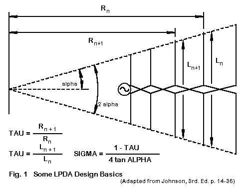
The antenna array consists of a series of dipoles whose self-resonant frequencies and lengths are set up in a periodic fashion and whose spacing is equally periodic. The elements are interconnected with a transmission line that reverses connections at each new dipole element, with the feedpoint normally at the junction with the shortest dipole of the array. We shall not dwell on the design parameters, since they appear in Johnson and Jasik as well as in the ARRL Antenna Book. Our concern will be limited to modeling LPDAs.
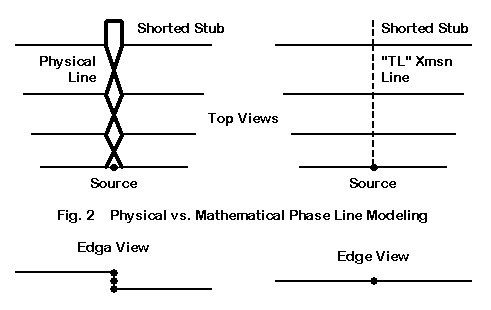
Essentially, we have two choices. We can attempt to model physically all aspects of the antenna array, as shown on the left in Fig. 2. Unfortunately, for NEC, this strategy quickly meets with some of the geometry limitations within the program. These limitations are functions of the calculation core and not of any particular implementation of NEC.
Since the elements are rarely of the same diameter as the transmission line wires, we encounter NEC's difficulties with angular junctions of dissimilar diameter wires. Results will rarely be accurate. Of course, every physical implementation of an LPDA has to deal with the crossing transmission line wires. The simplest scheme that works well appears in the left edge view. Let the inter-element transmission line (or phase line for short) be set up vertically. Then the left and right sides of each dipole can intersect alternate upper and lower wires of the phase line. The misalignment of up to a few inches of the two sides of the dipole will create no significant errors in the resulting antenna pattern or performance figures. However, the angular junction problem can only be overcome for a few designs using a constant diameter for all portions of the antenna.
MININEC (3.13) does not have the same angular junction limitation that troubles NEC, but MININEC does have limitations of its own. Sharp angular junctions require the use of high levels of segmentation or the use of length tapering to ensure that each junction is met with very short segment lengths. The short segment lengths minimize errors created by MININEC's tendency to "cut off" corners. The end result of overcoming the inherent MININEC limitation is a model that will overrun the maximum segment limitation of most versions of the program. Those programs that have extended the number of available segments will run very slowly with very high numbers of wires and segments in the model.
The most promising way to model an LPDA is to follow the lead of the right hand sketch in Fig. 2, which applies only to NEC (-2 or -4) models. Set up each dipole in its proper position. Use an odd number of segments on each dipole wire. (This note applies to the center wire of elements that have a tapered element diameter schedule, which in turn only applies to programs having corrections for NEC's difficulties with tapered diameter elements.)
From one dipole to the next, run a TL transmission line of the desired characteristic impedance. Reverse the connection of each transmission line installed. Place the source on the center of the shortest dipole. Many LPDA designs employ a shorted transmission line stub at the center of the longest element, and this can also be put in place in the model using the TL facility.
The following model description, adapted from a test file in EZNEC, illustrates the model construction principles.
17-10m Log Per - ARRL Ant Book          Frequency = 28  MHz.

Wire Loss: Aluminum -- Resistivity = 4E-08 ohm-m, Rel. Perm. = 1

              --------------- WIRES ---------------

Wire Conn.--- End 1 (x,y,z : in)  Conn.--- End 2 (x,y,z : in)  Dia(in) Segs

1          0.000,-163.46,  0.000         0.000,163.460,  0.000 1.25E+00  41
2         39.230,-130.76,  0.000        39.230,130.760,  0.000 1.00E+00  33
3         70.620,-104.62,  0.000        70.620,104.620,  0.000 7.50E-01  25
4         95.720,-83.690,  0.000        95.720, 83.690,  0.000 6.25E-01  21
5        115.810,-66.950,  0.000       115.810, 66.950,  0.000 5.00E-01  17

               -------------- SOURCES --------------

Source    Wire      Wire #/Pct From End 1    Ampl.(V, A)  Phase(Deg.)  Type
          Seg.     Actual      (Specified)

1           9     5 / 50.00   (  5 / 50.00)      1.000       0.000       I

                -------- TRANSMISSION LINES ---------

Line  Wire #/% From End 1   Wire #/% From End 1    Length    Z0   Vel Rev/
      Actual  (Specified)   Actual  (Specified)             Ohms Fact Norm

1    1/50.0  (  1/50.0)    2/50.0  (  2/50.0)  Actual dist  490.1  1.00  R
2    2/50.0  (  2/50.0)    3/50.0  (  3/50.0)  Actual dist  490.1  1.00  R
3    3/50.0  (  3/50.0)    4/50.0  (  4/50.0)  Actual dist  490.1  1.00  R
4    4/50.0  (  4/50.0)    5/50.0  (  5/50.0)  Actual dist  490.1  1.00  R
5    1/50.0  (  1/50.0)  Short ckt (Short ck)    6.000 in   490.1  1.00

Ground type is Free Space
Although this is a good illustration of the modeling technique, the model does not show exceptional performance.
Use of the TL facility avoids most of the difficulties of physically modeling the LPDA. However, the use of TL phasing lines has some limitations of its own. Theoretically, the phase line does not enter into the antenna's radiation on any frequency. However, physical placement of the stub can sometimes alter the antenna's performance on certain frequencies. As mathematical entities created by a network placed at a large distance from the antenna model proper, the TL phase line cannot show the potential effects of placement.
In addition, there are construction variables connected with the assembly of real LPDAs, and some of these cannot be captured by the suggested NEC modeling technique. For example, K4EWG presented a 20-10 meter LPDA in Vol. 3 of the ARRL Antenna Compendium. He used a number of interesting construction techniques, sketched in Fig. 3.
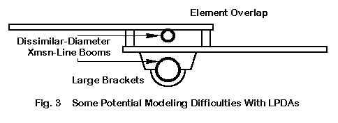
His phase line consisted of two tubes having different diameters. Ordinarily, the impedance of the line created by the two should be calculable from the diameter of the smaller tube, but the physical effects of the arrangement would be missing from the suggested modeling technique. In addition, he used muffler clamps to connect the lower element set to the larger boom. Most significant are the overlapping element ends--8" each side of center line. Overlapping the ends of dipole elements does affect antenna impedance in ways that the simplified model cannot fully capture.
For the most part, none of these construction techniques--and others that might be comparable--affects the antenna pattern with respect to gain, shape, or front-to-back ratio. When trying to model an LPDA using construction methods that have physical significance, it is important to establish before finalizing a model that these physical factors do not have distorting affects relative to the propose final model. You can do this by modeling individual elements with all physical aspect taken into account and comparing the results with simplified single elements.
Where constructed elements of the sort illustrated have their main effect is on the performance of the phase line. Its net effective impedance may not match the design impedance that we calculate from standard equations and simple round wires. The most straightforward way to deal with phase line variables is to survey the antenna performances at each check point using a variety of phase-line characteristic impedances from about 75-80 Ohms at the lower end of the spectrum to about 200-250 Ohms at the upper end.
The resulting chart of performance figures should include at least gain (initially done as free-space gain in dBi), front-to-back ratio, and source impedance. You may encounter phase-line characteristic impedance values that are more favorable to a smooth VSWR curve than other characteristic impedance values. You may also encounter interesting anomalies. For example, at one frequency within the antenna design range, gain may increase with the characteristic impedance, while at another frequency, the gain may increase inversely with increases in the characteristic impedance.
In short, do not expect a smooth set of performance figures that vary only slightly with variations in the phase-line characteristic impedance or frequency. Indeed, do not expect all resulting radiation patterns to closely resemble those obtained from Yagis. There is an old over-simplification that suggests that at any frequency, relative to the dipole that is closest to resonance, the elements affecting the overall antenna performance at that frequency are those immediately adjacent to the near-resonant dipole. Actually, at least two elements either side of the near-resonant dipole carry significant current and thus have major consequences for the resulting antenna radiation pattern. Since all of the elements carry at least some current, antenna patterns can vary significantly from the smoothly rounded norm that we have come to expect from Yagis.
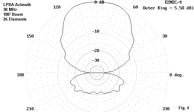
Fig. 4 shows one mild example, drawn from a model of a 3-30 MHz LPDA at 30 MHz. The array is 100' long and has 26 elements. Clearly apparent are the incipient lobes created by harmonic operation of elements distant from resonance at 30 MHz. Two extra notes are needed here. First, this is not the only type of pattern one might encounter. Diamond-shaped forward lobes are common. So, too, are split forward lobes with peaks separated from the center line by up to 20 degrees or so. Moreover, more than one of these effects may occur at once. Fortunately, most of the pattern aberrations do not occur on common single octave (for example, 20-10 meter) LPDAs of standard design.
Second, the characteristic impedance of the phase line has a bearing on the occurrence of these less-controlled azimuth pattern shapes. In general, the higher the impedance of the phase line, the smoother the outline of the azimuth pattern. However, the rear lobes may show some incipient lobes in the form of a slightly squared shape.
The gain reported by NEC is very likely to be less than the gain reported by designers who use some of the classic techniques associated with basic LPDA design instructions. The gain of an LPDA is a function of the value of Tau, one of the constants selected by the designer. Only values of Tau in the vicinity of 0.95 are capable of very high gain values, and only when these values are associated with very long boom lengths determined by an optimal value of the spacing constant, Sigma.
To see how this works, let us take a sample LPDA using 7 elements for 14 to 30 MHz and having a Tau of just over 0.85. We shall place these elements on three different booms of 20, 30, and 40 feet, respectively. These boom correspond to values of Sigma of 0.07, 0.10, and 0.14. The last value is closing in the optimum value one might calculate for Sigma (about 0.16). Although there are many ways of calculating potential gain in advance, Roger Cox, WB0DGF, reports in his program, LPCAD, that the gain values associated with the Tau of 0.85 should range from about 5.5 dBi to about 7.5 dBi. (Values are interpolated from his table.) We should expect the lower values to be associated with the shortest version of the antenna and the highest values to be connected to the longest version.
Here is a table of NEC-4 modeled results for the antenna. Gain is free-space gain in dBi, while front-to-back is the 180-degree ratio in dB. The shortest antenna uses a 75-Ohm phase line, while the longer models use 100-Ohm phase lines. All use a shorted stub from the longest element, and the stub is set to optimize performance and the feedpoint impedance.
          Gain/Front-Back Ratios of 7-Element LPDAs for 14-30 MHz
Boom Length         20'                 30'                 40'
  Frequency
     14         5.1 /  8.2          5.7 /  9.7          6.2 / 10.4
     18.12      5.8 /  9.8          7.3 / 13.1          7.2 / 22.6
     21         6.2 / 14.0          6.7 / 21.5          7.3 / 22.4
     24.95      6.3 / 16.8          6.6 / 17.2          7.5 / 27.9
     28         6.2 / 16.9          6.2 / 17.2          6.2 / 17.7
This table demonstrates several properties you are likely to see in LPDA designs of modest proportions. First, the longer the boom (up to the limits of optimal Sigma), the higher the gain for the same number of elements. Second, for any given design, some gain or front-to-back figures may well occur that are higher or lower than we would expect from smoothing the curve of results. For example, the 30' version gain at 18.12 MHz if higher than expected from the other values, and the feedpoint impedance turns out to be lower than expected at that frequency. Here is a case that might be "normalized" by adjustment of the length of the shorted stub--if that operation does not disturb performance on another frequency.
Third, performance at the upper and lower limits of the design range tends to fall off unless the LPDA is designed to have wider frequency limits surrounding the frequencies actually used. There appears to be a balance one might draw between too high an element density and too low a density. Higher densities tend to increase low frequency performance, but can actually detract from higher frequency performance when carried too far. Likewise, too low an element density can yield lower gain and front-to-back performance at the frequency limits of the design.
The present design does not correspond exactly with any published design, although it is related to several. It uses constant diameter elements--all 1" in diameter. Some designs may benefit from staggering the element diameters by increasing the values by the inverse of Tau, counting from the shortest element to the longest.
The table of values represents no judgment about the three variants of one design other than this: the values are typical of NEC reports and largely coincident with expectations raised by WB0DGF's suggested table. However, they are significantly lower than values we often see reported for LPDA designs in amateur literature. Therefore, each modeler who anticipates more than casual modeling of LPDA designs should model many designs and develop appropriate expectations for himself or herself.
We are often led to believe that LPDA antennas exhibit relatively smooth VSWR curves across the range of their design. If you model LPDAs, develop other expectations, as illustrated by Fig. 5.
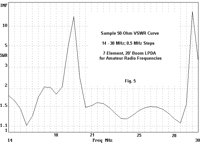
The SWR sweep in the graph is a function of NEC-4 calculations. Note that the SWR is well below 2:1 relative to a 50-Ohm standard for each of the amateur bands. While it modestly climbs above 2:1 at 17 and 17.5 MHz, it shows very major peaks in the 18.5 to 20 MHz range and again in the 29 to 29.5 MHz range. One of the functions of the shorted stub is to control the placement of the peaks so that the SWR is acceptable at the anticipated operating frequencies. Careful selection of the dipole lengths--as determined by the selection of the value for Tau--also contributes to lower SWR values at the desired frequencies.
As we lengthen the boom for the same set of elements, the SWR peaks decrease and the SWR becomes more manageable without critical adjustment to the value of Tau and the shorted stub. However, the curve will never be absolutely smooth. Moreover, the SWR value may never settle at a certain value, even when referenced to the most optimal impedance standard. What can happen with some designs is that the resistive component of the feedpoint impedance deviates most from the standard when the reactance is the lowest. Conversely, when the resistance is closest to the standard, the reactance reaches peak capacitive or inductive values. However, in some designs, the mean resistive component may shift as you move to different parts of the array's frequency range.
I have sampled some of the phenomena you may encounter when modeling LPDAs in order to remove some of the surprises that might shock a relatively inexperienced modeler out of further work with this kind of antenna design. Not all of the phenomena listed occur with every design--indeed, some designs will be very tame and well-controlled. However, the more phenomena with which you are acquainted, the less likely it will be that you will be discouraged from making optimizing adjustments to a model.
Nonetheless, even when you have achieved the best possible NEC model of an LPDA, expect to make field adjustments to compensate for construction factors that cannot be included in the model. NEC can be highly accurate in predicting the performance of a design, but it cannot adjust the shorted stub or decide for you whether or not to use a broad-band matching device between the antenna feedpoint and the coax.