
 LPCAD Designs and NEC Models of LPDAs
The log-periodic dipole array (LPDA) arouses amateur interest every so often. Based on a series of mathematical relationships, the LPDA design is amenable to computerized calculations for all element lengths and spacings. One program that has found wide use is LPCAD by Roger Cox, WB0DGF.
The point of this note is not to discuss basic LPDA design. This information can be found in the ARRL Antenna Book, Chapter 10, and in many standard antenna texts and references, for example, Kraus or Johnson and Jasik.
This note is devoted to a number of precautions we should take when moving from a page of design calculations, such as those produced by LPCAD, to a NEC model of the antenna design. To ease the transition, LPCAD provides a save function to capture the antenna design in standard NEC format (as well as in other formats). This model description will run on almost any version of NEC, -2 and above. Those having a version of EZNEC that translates from the .NEC format can import the file to that program.
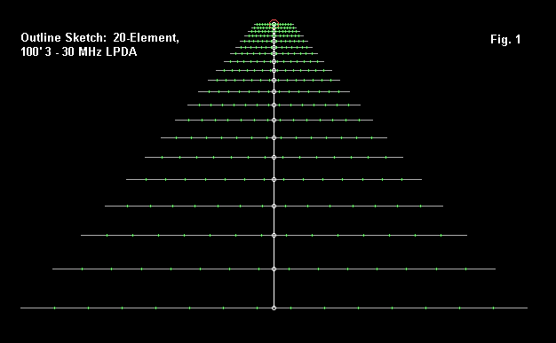
The save function is undoubtedly offered as a convenience to designers. However, the designer who models the antenna in NEC must take responsibility for ensuring that the model meets all of the requirements for being a good NEC model. Let's use an example: a 20-element 100' long 3-30 MHz LPDA of standard design. The value of Tau for this example is about 0.8737 and the value of Sigma is about 0.0409. Fig. 1 provides an outline of the general antenna design.
The LPCAD NEC file provides both a wires table and a TL transmission line table. The most accurate way to model LPDA designs that do not have unusual mechanical features, such as overlapping element ends, is to create each element at the correct spacing. Then use the TL facility of NEC-2 and higher to create the phasing line between each element pair, being sure to reverse connections of the line at each element. LPCAD adheres to this procedure in creating its NEC file.
The LPCAD NEC-file does not specify any wire loss, since material specifications are not used in the element calculations. Therefore, the first step for the modeler is to specify the wire material for the elements. Second, modeler should check the output azimuth plot specification. LPCAD uses a standard 10-degree step in the pattern, and the user may wish to reduce the step to 1 or 2 degrees to obtain smoother patterns with more detail.
With just these steps, an EZNEC description of the resulting file will look like the following listing.
20 el 100' 3-30 MHz                      Frequency = 3  MHz.

Wire Loss: Aluminum -- Resistivity = 4E-08 ohm-m, Rel. Perm. = 1

              --------------- WIRES ---------------

Wire Conn.--- End 1 (x,y,z : in)  Conn.--- End 2 (x,y,z : in)  Dia(in) Segs

1          0.000,-1003.7,  0.000         0.000,1003.68,  0.000 3.50E+00  15
2        164.166,-876.93,  0.000       164.166,876.934,  0.000 3.50E+00  15
3        307.601,-766.19,  0.000       307.601,766.193,  0.000 3.50E+00  15
4        432.923,-669.44,  0.000       432.923,669.437,  0.000 3.50E+00  15
5        542.419,-584.90,  0.000       542.419,584.899,  0.000 3.50E+00  15
6        638.087,-511.04,  0.000       638.087,511.037,  0.000 3.50E+00  15
7        721.675,-446.50,  0.000       721.675,446.503,  0.000 3.50E+00  15
8        794.707,-390.12,  0.000       794.707,390.118,  0.000 3.50E+00  15
9        858.516,-340.85,  0.000       858.516,340.853,  0.000 3.50E+00  15
10       914.267,-297.81,  0.000       914.267,297.810,  0.000 3.50E+00  15
11       962.978,-260.20,  0.000       962.978,260.202,  0.000 3.50E+00  15
12       1005.54,-227.34,  0.000       1005.54,227.343,  0.000 3.50E+00  15
13       1042.72,-198.63,  0.000       1042.72,198.634,  0.000 3.50E+00  15
14       1075.21,-173.55,  0.000       1075.21,173.550,  0.000 3.50E+00  15
15       1103.60,-151.63,  0.000       1103.60,151.634,  0.000 3.50E+00  15
16       1128.40,-132.49,  0.000       1128.40,132.485,  0.000 3.50E+00  15
17       1150.07,-115.75,  0.000       1150.07,115.755,  0.000 3.50E+00  15
18       1169.00,-101.14,  0.000       1169.00,101.137,  0.000 3.50E+00  15
19       1185.55,-88.365,  0.000       1185.55, 88.365,  0.000 3.50E+00  15
20       1200.00,-77.206,  0.000       1200.00, 77.206,  0.000 3.50E+00  15

               -------------- SOURCES --------------

Source    Wire      Wire #/Pct From End 1    Ampl.(V, A)  Phase(Deg.)  Type
          Seg.     Actual      (Specified)

1           8    20 / 50.00   ( 20 / 50.00)      0.707       0.000       V

No loads specified

                -------- TRANSMISSION LINES ---------

Line  Wire #/% From End 1   Wire #/% From End 1    Length     Z0   Vel Rev/
      Actual  (Specified)   Actual  (Specified)              Ohms Fact Norm

1    1/50.0  (  1/50.0)    2/50.0  (  2/50.0)  Actual dist  200.0  1.00  R
2    2/50.0  (  2/50.0)    3/50.0  (  3/50.0)  Actual dist  200.0  1.00  R
3    3/50.0  (  3/50.0)    4/50.0  (  4/50.0)  Actual dist  200.0  1.00  R
4    4/50.0  (  4/50.0)    5/50.0  (  5/50.0)  Actual dist  200.0  1.00  R
5    5/50.0  (  5/50.0)    6/50.0  (  6/50.0)  Actual dist  200.0  1.00  R
6    6/50.0  (  6/50.0)    7/50.0  (  7/50.0)  Actual dist  200.0  1.00  R
7    7/50.0  (  7/50.0)    8/50.0  (  8/50.0)  Actual dist  200.0  1.00  R
8    8/50.0  (  8/50.0)    9/50.0  (  9/50.0)  Actual dist  200.0  1.00  R
9    9/50.0  (  9/50.0)   10/50.0  ( 10/50.0)  Actual dist  200.0  1.00  R
10  10/50.0  ( 10/50.0)   11/50.0  ( 11/50.0)  Actual dist  200.0  1.00  R
11  11/50.0  ( 11/50.0)   12/50.0  ( 12/50.0)  Actual dist  200.0  1.00  R
12  12/50.0  ( 12/50.0)   13/50.0  ( 13/50.0)  Actual dist  200.0  1.00  R
13  13/50.0  ( 13/50.0)   14/50.0  ( 14/50.0)  Actual dist  200.0  1.00  R
14  14/50.0  ( 14/50.0)   15/50.0  ( 15/50.0)  Actual dist  200.0  1.00  R
15  15/50.0  ( 15/50.0)   16/50.0  ( 16/50.0)  Actual dist  200.0  1.00  R
16  16/50.0  ( 16/50.0)   17/50.0  ( 17/50.0)  Actual dist  200.0  1.00  R
17  17/50.0  ( 17/50.0)   18/50.0  ( 18/50.0)  Actual dist  200.0  1.00  R
18  18/50.0  ( 18/50.0)   19/50.0  ( 19/50.0)  Actual dist  200.0  1.00  R
19  19/50.0  ( 19/50.0)   20/50.0  ( 20/50.0)  Actual dist  200.0  1.00  R

Ground type is Free Space
Judging from some correspondence, many modelers would accept this model at face value as a proper model and proceed to check the performance at frequencies of interest. In fact, this model would show up as acceptable of better on the Average Gain Test, since this test does not pick up segmentation flaws unless they are wildly flagrant. However, there are two important modifications that one should make to this model before trusting any outputs.
First, the model is uniformly specified with 15 segments per wire throughout the 20 elements. However, every element is a different length. Hence, segmentation should vary from one element to the next. How many segments each element should have is a function of the length of the longest element and the highest frequency at which the antenna will operate. The longest element is a little over 2000" and the highest frequency is 30 MHz. We need conservatively about 10 segments per half wavelength, but because we shall place a transmission line along the exact center line of the antenna, we need for each element an odd number of segments. The requirement for an odd number of elements will limit the precision of our segmentation.
Since the longest element is a bit over 5 wl long at 30 MHz, let's assign 107 segments to the longest element. For each shorter element, in order, we simply multiply by Tau, using the preceding element answer as the basis for the next element. We shall have to round upward or downward to the closest odd number to obtain the segment number for the element in question. For the example in question, the shortest two elements each receive 9 segments, since their 1/2 wl resonant frequencies are above 30 MHz.
Second, consider the element diameter. The value in the diameter column is the average element diameter that the user specified as an input to the calculations. However, this value is very often not an accurate reflection of the intended element diameter for the actual antenna. Hence, we should replace the average diameter with value as close to reality as possible.
For the model in question, I specified a range of diameters from 0.5" for the shortest element to 6.5" for the longest. The design required that each element change according to Tau in the descent from 6.5" to 0.5". Once more, this is a simply matter of successive multiplication of preceding values by Tau to obtain the next smaller diameter. (The design purpose in this case was to have a constant element length-to-diameter ratio for the entire model. In any event, you should use element diameter values as close to reality as the stage of design will allow.)
The modified antenna model then took on this appearance.
20 el 100' 3-30 MHz                       Frequency = 3  MHz.

Wire Loss: Aluminum -- Resistivity = 4E-08 ohm-m, Rel. Perm. = 1

              --------------- WIRES ---------------

Wire Conn.--- End 1 (x,y,z : in)  Conn.--- End 2 (x,y,z : in)  Dia(in) Segs

1          0.000,-1003.7,  0.000         0.000,1003.68,  0.000 6.50E+00 107
2        164.166,-876.93,  0.000       164.166,876.934,  0.000 5.68E+00  93
3        307.601,-766.19,  0.000       307.601,766.193,  0.000 4.96E+00  81
4        432.923,-669.44,  0.000       432.923,669.437,  0.000 4.34E+00  71
5        542.419,-584.90,  0.000       542.419,584.899,  0.000 3.79E+00  63
6        638.087,-511.04,  0.000       638.087,511.037,  0.000 3.31E+00  55
7        721.675,-446.50,  0.000       721.675,446.503,  0.000 2.89E+00  47
8        794.707,-390.12,  0.000       794.707,390.118,  0.000 2.53E+00  41
9        858.516,-340.85,  0.000       858.516,340.853,  0.000 2.21E+00  37
10       914.267,-297.81,  0.000       914.267,297.810,  0.000 1.93E+00  31
11       962.978,-260.20,  0.000       962.978,260.202,  0.000 1.69E+00  27
12       1005.54,-227.34,  0.000       1005.54,227.343,  0.000 1.47E+00  25
13       1042.72,-198.63,  0.000       1042.72,198.634,  0.000 1.29E+00  21
14       1075.21,-173.55,  0.000       1075.21,173.550,  0.000 1.12E+00  19
15       1103.60,-151.63,  0.000       1103.60,151.634,  0.000 9.80E-01  17
16       1128.40,-132.49,  0.000       1128.40,132.485,  0.000 8.60E-01  15
17       1150.07,-115.75,  0.000       1150.07,115.755,  0.000 7.50E-01  13
18       1169.00,-101.14,  0.000       1169.00,101.137,  0.000 6.50E-01  11
19       1185.55,-88.365,  0.000       1185.55, 88.365,  0.000 5.70E-01   9
20       1200.00,-77.206,  0.000       1200.00, 77.206,  0.000 5.00E-01   9

              -------------- SOURCES --------------

Source    Wire      Wire #/Pct From End 1    Ampl.(V, A)  Phase(Deg.)  Type
          Seg.     Actual      (Specified)

1           5    20 / 50.00   ( 20 / 50.00)      0.707       0.000       V

No loads specified

                -------- TRANSMISSION LINES ---------

Line  Wire #/% From End 1   Wire #/% From End 1    Length     Z0   Vel Rev/
      Actual  (Specified)   Actual  (Specified)              Ohms Fact Norm

1    1/50.0  (  1/50.0)    2/50.0  (  2/50.0)  Actual dist  200.0  1.00  R
2    2/50.0  (  2/50.0)    3/50.0  (  3/50.0)  Actual dist  200.0  1.00  R
3    3/50.0  (  3/50.0)    4/50.0  (  4/50.0)  Actual dist  200.0  1.00  R
4    4/50.0  (  4/50.0)    5/50.0  (  5/50.0)  Actual dist  200.0  1.00  R
5    5/50.0  (  5/50.0)    6/50.0  (  6/50.0)  Actual dist  200.0  1.00  R
6    6/50.0  (  6/50.0)    7/50.0  (  7/50.0)  Actual dist  200.0  1.00  R
7    7/50.0  (  7/50.0)    8/50.0  (  8/50.0)  Actual dist  200.0  1.00  R
8    8/50.0  (  8/50.0)    9/50.0  (  9/50.0)  Actual dist  200.0  1.00  R
9    9/50.0  (  9/50.0)   10/50.0  ( 10/50.0)  Actual dist  200.0  1.00  R
10  10/50.0  ( 10/50.0)   11/50.0  ( 11/50.0)  Actual dist  200.0  1.00  R
11  11/50.0  ( 11/50.0)   12/50.0  ( 12/50.0)  Actual dist  200.0  1.00  R
12  12/50.0  ( 12/50.0)   13/50.0  ( 13/50.0)  Actual dist  200.0  1.00  R
13  13/50.0  ( 13/50.0)   14/50.0  ( 14/50.0)  Actual dist  200.0  1.00  R
14  14/50.0  ( 14/50.0)   15/50.0  ( 15/50.0)  Actual dist  200.0  1.00  R
15  15/50.0  ( 15/50.0)   16/50.0  ( 16/50.0)  Actual dist  200.0  1.00  R
16  16/50.0  ( 16/50.0)   17/50.0  ( 17/50.0)  Actual dist  200.0  1.00  R
17  17/50.0  ( 17/50.0)   18/50.0  ( 18/50.0)  Actual dist  200.0  1.00  R
18  18/50.0  ( 18/50.0)   19/50.0  ( 19/50.0)  Actual dist  200.0  1.00  R
19  19/50.0  ( 19/50.0)   20/50.0  ( 20/50.0)  Actual dist  200.0  1.00  R
20   1/50.0  (  1/50.0)  Short ckt (Short ck)   90.000 in   200.0  1.00

Ground type is Free Space
Besides the changes to the element segments and element diameter columns, one other addition to the model is evident. I added a shorted transmission line stub to the phasing line at the rearmost element. Actually, I ran this model with and without the stub to see the difference in performance at selected frequencies.
Notice that the stub has a specific length and is not the oft-used 1/4 wl (or the length of 1/2 the longest element). The stub was chosen to improve low frequency performance while having the least effect on upper frequency performance.
The modification significantly increase the segment count for the entire model (with or without the stub). The example above uses 792 segments, which may be beyond the common 500-segment limit of many entry-level NEC programs. However, it is the minimal satisfactory model of the LPDA design in question. In fact, convergence testing should check the model up to at least 1.5 times the segmentation density used here. (See the end of this note for the convergence test.)
Is all this really necessary? To find out, let's run frequency sweeps of the original model (with the aluminum elements and smaller plot step level in place) and of the two modified models (without and with a stub). If the original model formulation is satisfactory, then its curves should track the curves of the modified models except for any stub effects. As a preliminary set of checks, let's plot the following parameters: free-space gain in dBi, 180-degree front-to-back ratio in dB, source resistance in Ohms, source reactance in Ohms, and VSWR relative to some standard.
For a real design, we would run detailed frequency sweeps across each intended band of operation. For this general profile, we can use a sweep that checks the values of interest at 1 MHz intervals from 3 through 30 MHz, the design range of the model. In the following graphs, "20100" refers to the unmodified model, "20100A" refers to the stubless modified model, and "20100ATL" refers to the modified model with a shorted stub.
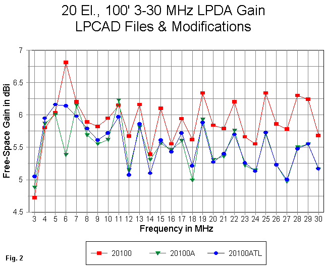
Fig. 2 provides graphs of the gain values for the three models. Except for the 6 MHz region, the stub and no-stub modified models track each other very well, with the stub model having the highest gain at 3 MHz. The original model using a constant 15-segments per element erroneously predicts a gain peak at 6 MHz. More significantly, above about 12 MHz, the original model provides significantly over-optimistic values for the gain of the antenna, a typical result of inadequate segmentation. However, note that the values occur in the frequency region in which we might think that the segmentation is adequate. This is a lesson to the effect that all of the elements of an LPDA design play a role at all frequencies.
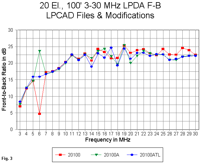
In Fig. 3, we see the generally coincident curves for all three models with respect to front-to-back ratio. The original model is once more a bit over-optimistic at the highest frequencies, but these high reports are confined to the 25 to 29 MHz region. The most serious anomaly is at 6 MHz, where the original model predicts a very low front-to-back ratio (the same frequency on which it predicted an unusually high gain value). The stubless model that corresponds to the initial model (which is also without a shorted stub) predicts exactly the opposite--an unusually high front-to- back ratio. Addition of the stub smooths the curve considerably.
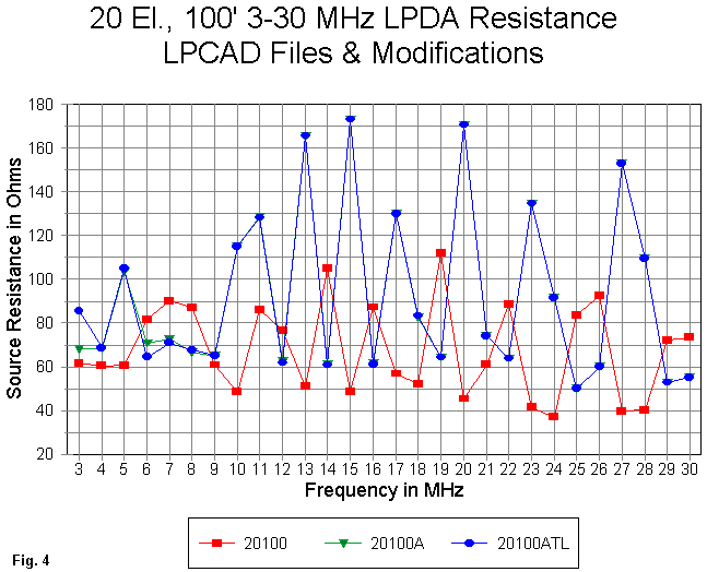
When we turn to the resistance and reactance components (Fig. 4 and Fig. 5) of the source impedance, the odd performance of the original model shows itself most vividly. The curves for the stub and stubless models are so close together above the lowest region of the passband that one curve obscures the other. This phenomenon makes all the more evident that fact that the initial model tends to dip and peak in a rhythm directly opposite that of the more adequately segmented model. The resistance values reported by the 15- segment per element model would have to be accounted wholly unreliable.
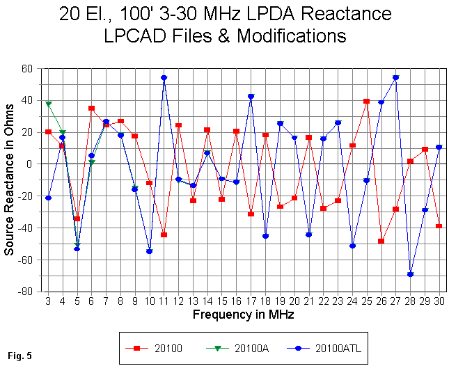
The graph of reactance values tells a very similar story. Again, the stubbed and stubless models coincide above the lowest frequencies, but the initial model fails to track these curves. In fact, it tends to take just the opposite turn. It is well to remember that the larger model more closely approaches convergence than the smaller model and hence must be accounted a more proper model of the antenna than the smaller model.
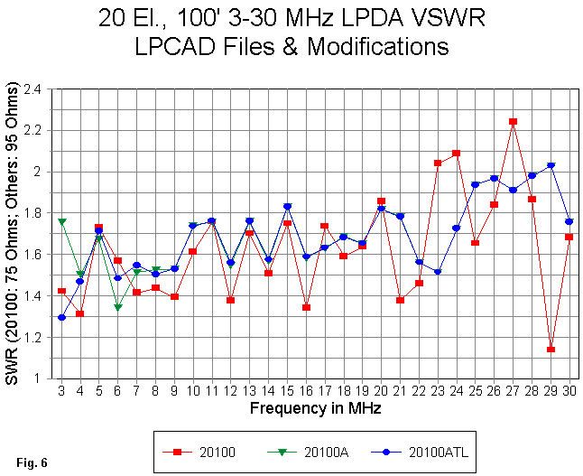
Because the resistance and reactance values were at such odds, it was necessary to track VSWR against different reference values in Fig. 6. The initial model used a 75-Ohm standard, suggesting that it might be directly fed with a coaxial cable. However, both larger models are referenced to 95 Ohms, a value taken as close to the mean between the extremes of the resistive components of the source impedance. Incidentally, the LPCAD prediction for a source impedance is 103 Ohms.
The importance of the difference in VSWR reference standards lies in the consequences for designing the impedance matching required for connecting a main feedline to the antenna. The initial model's prediction that a 75-Ohm cable would be sufficient is unlikely to be fulfilled. More likely is the potential for using a wide-band 2:1 impedance matching device to connect the antenna to a 50-Ohm cable.
The inadequacies of uncritically adopting the transfer model as a proper NEC model are all too evident from the comparative graphs. This is not a criticism of LPCAD, since the main function of saving the LPDA design as a NEC model is to release the designer from the tedium of entering every element length, space, and transmission line without omission, slippage, or transposition of numbers. However, it remains the responsibility of the modeler to use sufficient care to ensure that the resulting model meets all applicable NEC standards for being a proper model within the guidelines for the core. If a model turns out to be too big for the limits of a software package, it is dangerous to trust the results of a model squeezed down in segmentation to fit those limits. Instead, the model needs to be whatever size is required for it to yield reliable results--and sometimes, that calls for a software package with larger limits. Most especially, models should never be shrunken just to reduce the time it takes to make a set of runs.
Programs like LPCAD are exceptionally useful design tools. However, like NEC itself, they have limitations. When using them, it pays to find and understand those limitations so that they do not impede design progress. Translating LPCAD designs into NEC models is a fascinating case in point.
In the present case, we are dealing with relatively large models--relative, that is, to normal amateur radio modeling practices, although these models would be small in the confines of some engineering projects. The modified models--with and without a stub--have 792 segments overall, distributed in 20 elements. A reasonable convergence test might add 50% to that number as a basic convergence check.
However, the segmentation of the model must meet special requirements. The number of segments per element is determined by a rolling Tau calculation starting from the longest element. The calculation is then rounded to the nearest odd-number of segments. To avoid double rounding errors, I performed the Tau-based calculations, beginning with 161 segments on the rear element, up from 107 on the models considered above. The result appears in the partial model description below:
              --------------- WIRES ---------------

Wire Conn.--- End 1 (x,y,z : in)  Conn.--- End 2 (x,y,z : in)  Dia(in) Segs

1          0.000,-1003.7,  0.000         0.000,1003.68,  0.000 6.50E+00 161
2        164.166,-876.93,  0.000       164.166,876.934,  0.000 5.68E+00 141
3        307.601,-766.19,  0.000       307.601,766.193,  0.000 4.96E+00 123
4        432.923,-669.44,  0.000       432.923,669.437,  0.000 4.34E+00 107
5        542.419,-584.90,  0.000       542.419,584.899,  0.000 3.79E+00  93
6        638.087,-511.04,  0.000       638.087,511.037,  0.000 3.31E+00  81
7        721.675,-446.50,  0.000       721.675,446.503,  0.000 2.89E+00  71
8        794.707,-390.12,  0.000       794.707,390.118,  0.000 2.53E+00  63
9        858.516,-340.85,  0.000       858.516,340.853,  0.000 2.21E+00  55
10       914.267,-297.81,  0.000       914.267,297.810,  0.000 1.93E+00  47
11       962.978,-260.20,  0.000       962.978,260.202,  0.000 1.69E+00  41
12       1005.54,-227.34,  0.000       1005.54,227.343,  0.000 1.47E+00  37
13       1042.72,-198.63,  0.000       1042.72,198.634,  0.000 1.29E+00  31
14       1075.21,-173.55,  0.000       1075.21,173.550,  0.000 1.12E+00  27
15       1103.60,-151.63,  0.000       1103.60,151.634,  0.000 9.80E-01  25
16       1128.40,-132.49,  0.000       1128.40,132.485,  0.000 8.60E-01  21
17       1150.07,-115.75,  0.000       1150.07,115.755,  0.000 7.50E-01  19
18       1169.00,-101.14,  0.000       1169.00,101.137,  0.000 6.50E-01  17
19       1185.55,-88.365,  0.000       1185.55, 88.365,  0.000 5.70E-01  15
20       1200.00,-77.206,  0.000       1200.00, 77.206,  0.000 5.00E-01  13
I then took a long walk while I frequency swept the enlarged model from 3 to 30 MHz in 1 MHz steps. The results were then entered into a spreadsheet. Differentials between the values for the smaller and the larger model covered gain and front-to-back ratio (in dB), source resistance and reactance (in Ohms), and 95-Ohm VSWR. The results form the basis for a judgment of whether the smaller model is sufficiently converged with the larger to be considered reliable.
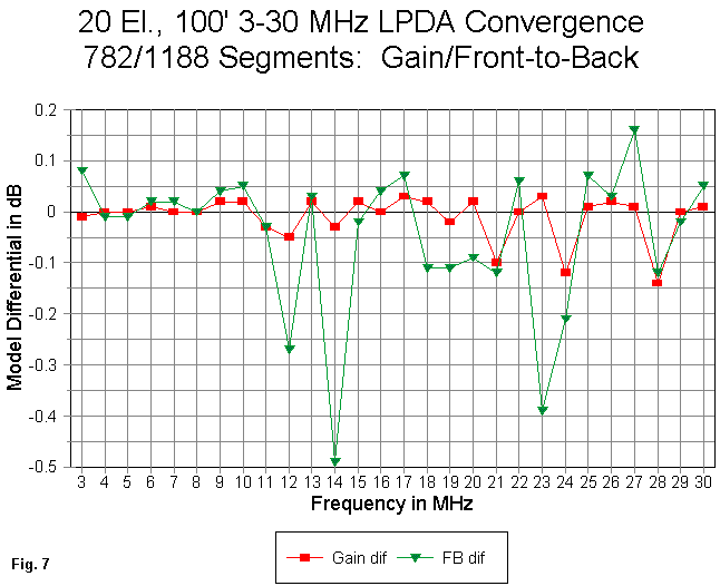
Fig. 7 shows the differentials for gain and front-to-back ratio. The maximum gain difference is under 0.15 dB or less than 3% of the average gain. The maximum front-to-back differential is 0.49 dB, again, less than 3% of the average front-to-back level.
Whether these numbers represent significant differences is a question of judgment related to the purposes for which one is doing the modeling. A gain difference of 0.15 dB is certainly not operationally detectable. Nor is a front-to-back differential of 0.49 dB. Since these maximum figures do not represent a general trend in the curves, they are unlikely to be meaningful for any design work one might do on an antenna of this sort. In fact, the most notable fact about the two curves in Fig. 7 is how closely they coincide, that is, how much of the curves remains within +/-.05 dB of zero.
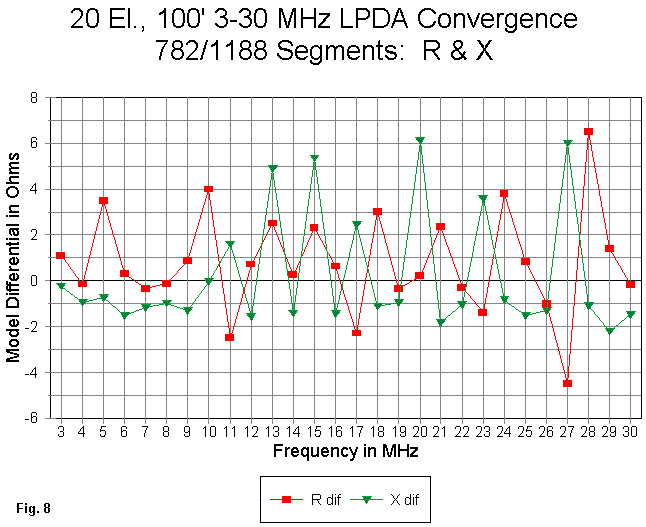
The resistance and reactance curves appear in Fig. 8. The maximum resistance and reactance deviations are about 6 Ohms each, within 5% of the total range of values for each parameter. What the graph of differences cannot show is that differences are largest where the values compared are large. The resistance ranges from about 49 Ohms to over 170 Ohms, and the 6-Ohm peaks occur with the largest values. Likewise, reactance ranges from about -55 Ohms to nearly +70 Ohms, and once more, peak differences attach to the highest values. We may have noticed that in the progression of source impedance values for an LPDA, most instances of high reactance occur when the resistance is most distant from its mean value. Hence, the resistance and reactance peak values appear at different points on the basic graphs.
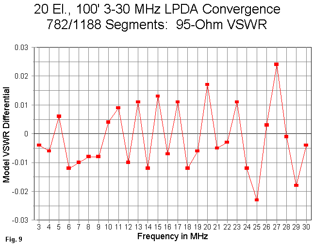
The result is a 95-Ohm VSWR graph of differences (Fig. 9) that peaks at values less than 0.025, a truly insignificant differential for any operational antenna consideration with which I am acquainted.
The general conclusion one might reach here is that the smaller model converges well with the larger and may be considered reliable for most purposes. This kind of test--and the results--give confidence that the graphed results for the modified models are far more usable than those for the unmodified model using a standard 15 elements per element.
Nevertheless, the general conclusion represents a "smoothed" judgment. There are still a few values on the difference graphs that call attention to themselves. In such cases, we may usefully do two things: 1. We can keep our eye out in further modeling for significant anomalies that occur at the same frequencies. 2. Should we implement the design used for discussion here, we might make a few special checks at these frequencies during the field testing and adjustment to ensure that operational values do not exceed whatever limits might be specified in the final design.
You will not. There will be slight differences in the two designs. As an example, here are the element descriptions for two LPDAs, the first designed by entering a Tau of 0.85 and a Sigma of 0.04. The second design was derived by entering 7 elements and 294.185" as the length, both figures taken from the first design. The frequency range for the design is 6.8 to 15 MHz.
1.  Designed with Tau = 0.85; Sigma = 0.04
              --------------- WIRES ---------------

Wire Conn. --- End 1 (x,y,z : in)  Conn. --- End 2 (x,y,z : in)   Dia(in) Segs

1            0.000,-442.80,  0.000         0.000,442.800,  0.000 1.00E+00  29
2           70.848,-376.38,  0.000        70.848,376.380,  0.000 1.00E+00  25
3          131.069,-319.92,  0.000       131.069,319.923,  0.000 1.00E+00  21
4          182.257,-271.93,  0.000       182.257,271.935,  0.000 1.00E+00  17
5          225.766,-231.14,  0.000       225.766,231.144,  0.000 1.00E+00  15
6          262.749,-196.47,  0.000       262.749,196.473,  0.000 1.00E+00  13
7          294.185,-167.00,  0.000       294.185,167.002,  0.000 1.00E+00  11

2.  Designed with 7 Elements and 294.185" Length
              --------------- WIRES ---------------

Wire Conn. --- End 1 (x,y,z : in)  Conn. --- End 2 (x,y,z : in)   Dia(in) Segs

1            0.000,-442.80,  0.000         0.000,442.800,  0.000 1.00E+00  29
2           72.738,-371.50,  0.000        72.738,371.495,  0.000 1.00E+00  25
3          133.763,-311.67,  0.000       133.763,311.673,  0.000 1.00E+00  21
4          184.961,-261.48,  0.000       184.961,261.484,  0.000 1.00E+00  17
5          227.915,-219.38,  0.000       227.915,219.377,  0.000 1.00E+00  15
6          263.951,-184.05,  0.000       263.951,184.050,  0.000 1.00E+00  13
7          294.185,-154.41,  0.000       294.185,154.413,  0.000 1.00E+00  11
The calculated values for the second design are Tau = 0.840 and Sigma = 0.041. These small changes result in a 10" shortening of the second element (the prime current carraier at the low end of the passband) and a 26" shortening of the 7th element. These changes are not minor, as Fig. 10 demonstrates.
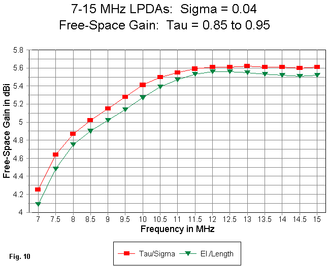
Lowering the value of Tau shortens every element in the array except the rear one. One consequence is to lower gain everywhere in the passband. Whether the amount is significant is a user judgment based on design goals. However, it is sufficient to be noticable and designers should be alerted to this facet of LPCAD operation.
Updated 09-26-99; 10-7-99. © L. B. Cebik, W4RNL. Data may be used for
personal purposes, but may not be reproduced for publication in print or
any other medium without permission of the author.