
 So You Want to Build Your Own LPDA
In Part 1 of this series, we looked at the effects of varying Tau and Sigma (over a limited range of samples) and at some short-boom LPDAs. All of the designs used standard calculation techniques. In addition, each was assigned a 200-Ohm inter-element phasing line, according to general recommendations. Since our frequency range for the exercise is 7 to 15 MHz, we selected a standard 1" uniform diameter for every element of every design. The only concession we made to improvement was to decrease the lower design frequency from the 7 MHz operational limit to 6.8 MHz to ensure a reasonable gain at the low end of the passband.
In this part of the exercise, let's explore some of the means that might be used to improve the performance of a basic LPDA design. We shall explore each technique individually, rather than try from the start to develop an optimized design. Our goal will be to understand the likely amount and type of improvement that each technique offers. In practice, optimizing an LPDA design with all of the factors involves many iterations, each making a small adjustment in one or more of the possible improvement factors until one reaches a peak performance level or ends the process in exhaustion.
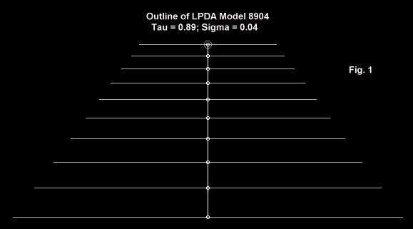
We should make each effort comparable, so that we can distinguish major advances from minor ones. One step in this direction is to select from the models in Part 1 a single design that might benefit from the efforts. My choice is model 8904, a 10-element LPDA that is 34.87' long with a Tau of 0.89 and a Sigma of 0.04. Fig. 1 provides the general outline.
For most of the efforts, the dimensions of this design will not change. It will retain throughout the same lengths with the same elements spacing (with one or two clearly announced exceptions). Hence, the following description will suffice for almost all of our work.
8904C                      EZNEC/4  ver. 2.5

6.8-15 MHz .89/.04                           10-08-1999     09:18:15

Frequency = 7  MHz.

Wire Loss: Aluminum -- Resistivity = 4E-08 ohm-m, Rel. Perm. = 1

              --------------- WIRES ---------------

Wire Conn.--- End 1 (x,y,z : in)  Conn.--- End 2 (x,y,z : in)  Dia(in) Segs

1          0.000,-442.80,  0.000         0.000,442.800,  0.000 2.85E+00  31
2         70.848,-394.09,  0.000        70.848,394.092,  0.000 2.54E+00  27
3        133.903,-350.74,  0.000       133.903,350.742,  0.000 2.26E+00  25
4        190.021,-312.16,  0.000       190.021,312.160,  0.000 2.01E+00  23
5        239.967,-277.82,  0.000       239.967,277.823,  0.000 1.79E+00  19
6        284.419,-247.26,  0.000       284.419,247.262,  0.000 1.59E+00  17
7        323.981,-220.06,  0.000       323.981,220.063,  0.000 1.42E+00  15
8        359.191,-195.86,  0.000       359.191,195.856,  0.000 1.26E+00  13
9        390.528,-174.31,  0.000       390.528,174.312,  0.000 1.12E+00  13
10       418.418,-155.14,  0.000       418.418,155.138,  0.000 1.00E+00  11

              -------------- SOURCES --------------

Source    Wire      Wire #/Pct From End 1    Ampl.(V, A)  Phase(Deg.)  Type
          Seg.     Actual      (Specified)

1           6    10 / 50.00   ( 10 / 50.00)      0.707       0.000       V

No loads specified

                -------- TRANSMISSION LINES ---------

Line  Wire #/% From End 1   Wire #/% From End 1    Length     Z0   Vel Rev/
      Actual  (Specified)   Actual  (Specified)              Ohms Fact Norm

1    1/50.0  (  1/50.0)    2/50.0  (  2/50.0)  Actual dist  200.0  1.00  R
2    2/50.0  (  2/50.0)    3/50.0  (  3/50.0)  Actual dist  200.0  1.00  R
3    3/50.0  (  3/50.0)    4/50.0  (  4/50.0)  Actual dist  200.0  1.00  R
4    4/50.0  (  4/50.0)    5/50.0  (  5/50.0)  Actual dist  200.0  1.00  R
5    5/50.0  (  5/50.0)    6/50.0  (  6/50.0)  Actual dist  200.0  1.00  R
6    6/50.0  (  6/50.0)    7/50.0  (  7/50.0)  Actual dist  200.0  1.00  R
7    7/50.0  (  7/50.0)    8/50.0  (  8/50.0)  Actual dist  200.0  1.00  R
8    8/50.0  (  8/50.0)    9/50.0  (  9/50.0)  Actual dist  200.0  1.00  R
9    9/50.0  (  9/50.0)   10/50.0  ( 10/50.0)  Actual dist  200.0  1.00  R

Ground type is Free Space
You may note that the element diameters are not uniform. That will be one of our exercises. However, it is easy enough to substitute any desired element diameter for any element in the set (including our standard 1" diameter) All models use aluminum elements.
One strategy for increasing element diameter is simply to increase all element diameters by the same amount. Since our original designs specified 1" diameter elements, we might check performance with 2" diameter elements. We are here more interested in the degree of improvement we might obtain than with the question of how easily we might implement the change. Elements with an average diameter of 2" at 7 MHz are heavy under any design, and they present stress loads to the central boom of the design.
A second strategy we might try is to taper the element diameters. Although we could start with an arbitrary scheme, one effective way to ensure that elements have the same length-to-diameter ratio throughout the design is to use the value of Tau. If we set a diameter for the shortest elements, we may simply increase the diameter of each longer element by the inverse of Tau (sometimes called k or Kappa). The inverse of 0.89 is 1.1235955. . .. If we limit the precision to 2 decimal places, the tapered elements have the diameters shown in the model description above. The length-to-diameter ratio is a little over 310:1.
These are enough changes to make at one time, so let's explore the results.
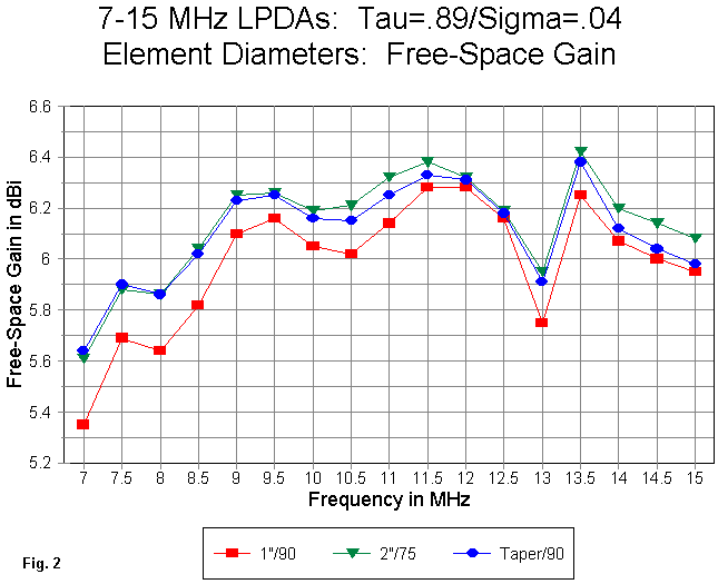
Fig. 2 shows the free-space gain in dBi of the three models with 1", 2", and tapered-diameter elements, respectively. Note that the curves generally track each other, coming together in the 12-12.5 MHz region of the passband. In general, the fatter elements add between 0.25 and 0.5 dB gain to the array. Except for the top two MHz of the passband, the tapered-element design general tracks the constant 2" design in gain performance.
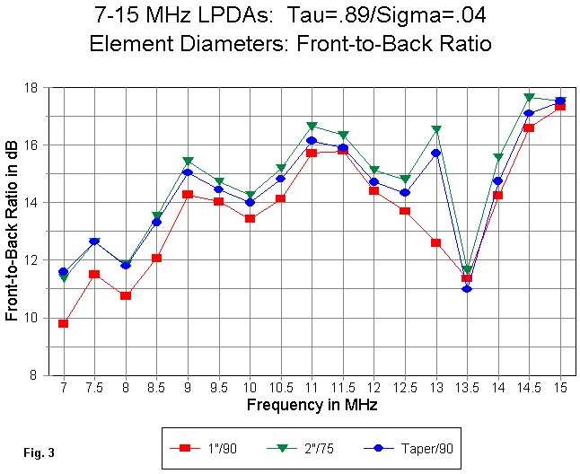
The front-to-back performance of the three models appears in Fig. 3. Once more, the 3 curves track each other with one major exception. In the 12 to 13.5 MHz range, the 1" diameter model shows a continuous decrease in front- to-back ratio, while the two designs with larger elements show a single sharp dip. Both of the larger-diameter models add about 1.5 dB to the front-to-back ratio at the low end of the passband, where it is naturally the lowest.
One of the reasons for selecting model 8904 as our subject was the existence of the gain and front-to-back ratio dip. The dip is not fatal to array operation, as the SWR curves remain within limits in the 13-14 MHz region of the passband. Moreover, the decrease in value does not extend below the lowest values for the entire passband. But it is still a problem if one of the design goals is the most even performance we can attain across the entire passband.
All three models are subject to harmonic operation of the rear-most elements within a critical frequency region of the passband. Where that mode of operation occurs most drastically is indicated by the frequency difference between the lowest gain and the lowest front-to-back ratio. We should look in the vicinity of about 13.25 MHz.
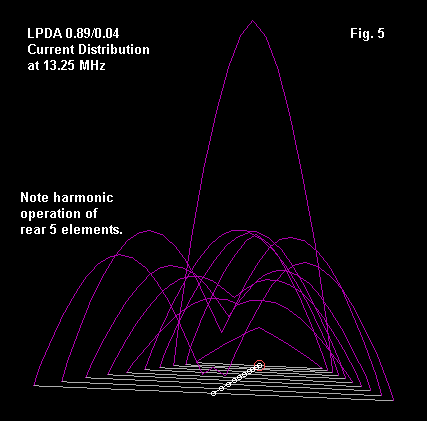
Fig. 5 shows the current distribution (and relative magnitudes) for the stubless tapered-diameter array at 13.25 MHz. Note that only the forward 5 elements show a single gain peak. The rear 5 elements all show the double hump of harmonic operation. (If the words were not so long, we could label the difference as that between dromedary and bactrian operation.) In LPDA operation, suppression of harmonic operation of elements is normally desired as a means to smooth the performance across the passband. So let's suppress it.
For the 1-octave LPDA, a simple shorted transmission line stub is sufficient to alter the impedances of the longest elements in the critical frequency region so that harmonic operation of the element does not occur. With a stub, element currents remain too low for the pattern of the array to be altered from its norm at the critical frequency region. Almost any stub length of moderate proportions will do the job. Generally, higher impedance stubs are preferred to lower impedance stubs, since they can be shorter for the same reactance level. However, some lengths are better than others.
To find the right stub length in a model simply means trying various lengths and watching the performance figures over the critical region of the passband. In my trials for 8904 with the tapered diameter elements, I examined lengths ranging from 36" down to 3" while checking performance at half-MHz intervals from 12.5 to 15 MHz. Here, in tabular form, is a portion of the survey. The figures shown are free-space gain in dBi and the front-to-back ratio in dB.
Freq                     8904C Stub length in inches
(MHz)          36"                 18"                 6"
12.5      6.09 / 15.54        6.08 / 15.65        6.08 / 15.75
13.0      5.99 / 15.44        6.00 / 15.35        6.00 / 15.27
13.5      5.95 / 15.53        5.97 / 15.35        5.99 / 15.11
14.0      5.97 / 15.57        6.00 / 15.45        6.01 / 15.11
14.5      6.01 / 15.16        6.03 / 15.75        6.03 / 15.95
15.0      6.02 / 13.63        6.01 / 15.89        6.00 / 16.33
There is nothing dramatic in the differences among stub lengths, although the shortest stub length shown does, on average, promise to outperform longer lengths. Nevertheless, field trimming the stub, however it might be implemented, is far from a tedious job, since any approximation would be indistinguishable in operation from any other.
The dramatic changes in performance come from comparing the same model, both with and without the stub.
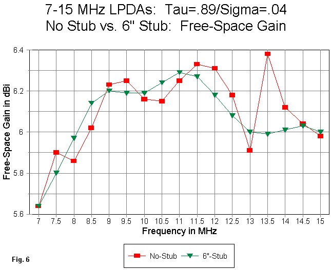
Fig. 6 provides the free-space gain curves for the stubless and stubbed models of 8904. If we say that the gain from 13 to 15 MHz now makes a smooth curve, we have only begun to notice significant differences in the curves. The addition of the stub has also altered the number and frequency placement of gain peaks across the passband. With the stub, we find peaks at 9, 11, and 14.5 MHz. Without the stub, we noticed peaks at 7.5, 9.5, 11.5, and 13.5 MHz. The 2 MHz interval between peaks in the stubless model has been replaced with peaks showing far less of an obvious pattern.
In exchange for the smoothness of the curve, we lost some interesting gain peaks. In a 1/2-scale version of the antenna, gain would be less at both 21 and 28 MHz. Nevertheless, given the variables of construction, we might find that the gain nulls might just move from the modeled positions to less desirable ones. Hence, a smooth curve is a major goal wherever it can be achieved.
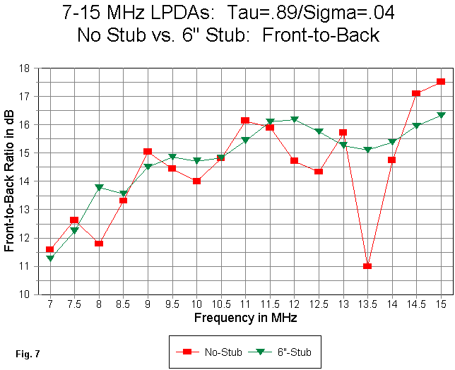
The front-to-back ratio curves in Fig. 7 also show the same curve displacement that we saw in the gain curves. However, note that gain and front-to-back ratio do not peak for most designs at the same frequencies. When we spot unnaturally large peaks on the same or adjacent check frequencies, we should examine the design for harmonic operation of some elements.
The stubbed model has peaks at 8, 9.5, and 12 MHz, with a possible peak at 15 MHz. The placement is about a half MHz higher than the corresponding gain peaks. In the unstubbed model, peaks occur at 7.5, 9, 11, 13, and 15 MHz, in almost all cases, about a half-MHz below the gain-peak frequencies. There are further refinements to the development of these curves that the profile intervals cannot display, but this much should suffice to show the power of a stub to move performance peaks and valleys around, while smoothing the curve overall. I suppose we should note in passing that the deep front-to-back dip at 13.5 MHz is missing from the stubbed curve.
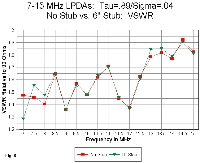
The SWR curves, shown in Fig. 8, provide evidence that an optimized stub for an LPDA array has minimal effect on the overall SWR performance of the antenna. As we might expect, the stub does alter the source resistance and reactance at the lowest frequencies, where peak current magnitudes involve the longest elements--where the stub is attached. A second region of source impedance change is in the critical frequency region. Outside of these two regions, the SWR curves for the stubbed and unstubbed models track each other closely.
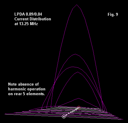
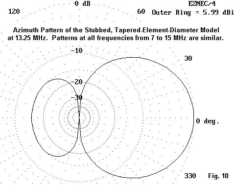
For the record, we might record what is now happening at 13.25 MHz, the frequency at which we examined the current distribution and magnitude on the elements of the 8904C LPDA array. As Fig. 9 shows, the addition of the 6" stub brings the rear 5 elements into relative quiescence so that the forward 5 elements take almost complete control of the antenna pattern. And while we are recording for the record, Fig. 10 shows the azimuth pattern of the stubbed array at 13.25 MHz. The pattern is perfectly ordinary for an array of this size and all of the patterns at all of the frequencies look almost identical. That is why we added the stub.
Many LPDA designs--for example, those intended for use on the amateur band only--do not care about having smooth performance curves across a given pass band. Instead, they wish to optimize performance within specific passband segments. Since we can control wayward performance in critical frequency regions with a stub, we can often obtain good ham band performance, but at the expense of performance outside those primary frequencies.
Lowering the inter-element phaseline characteristic impedance can increase the harmonic operation of the rearward elements. Therefore, there is a certain "danger" in designing with a lower phaseline impedance. Nonetheless, the appeal of more gain and possibly a higher front-to-back ratio makes this strategy appeal to designers.
Our prime model, 8904, is actually not a good candidate for this use. The performance increase, while notable on a graph, will not be very operationally significant. LPDAs with higher values of Tau tend to show better results. Nonetheless, rather than confuse matters by introducing wholly new designs, let's see what happens with old 8904.
We shall begin with the initial model that used 1" elements throughout.
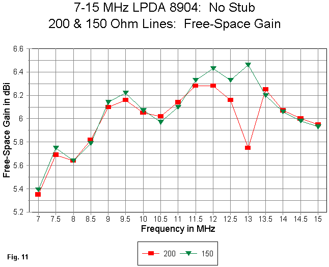
See Fig. 11. If we reduce the phaseline impedance to 150 Ohms, the 1" model acquires a little free-space gain at most frequencies, along with a gain peak at 13 MHz, rather than the original dip. There are a few places in the spectrum where the original 200-Ohm model surpasses the 150-Ohm model in gain, such as 8.5, 10.5, and above 13.5 MHz. In fact, for all of the comparisons in this section, we shall discover that with standard design element lengths and spacings, the lower the phaseline impedance, the lower the upper-end gain.
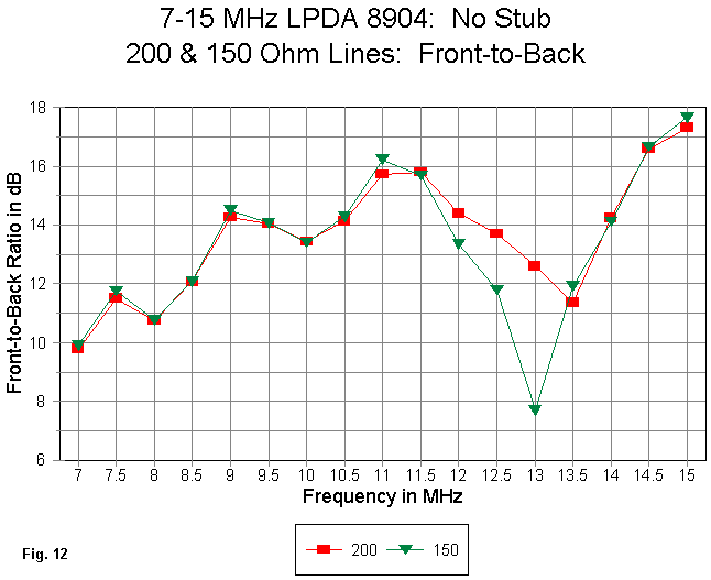
Before we cheer too loudly over the gain peaks in Fig. 11, we should examine Fig. 12, the graph of front-to-back ratios for the 200-Ohm and 150- Ohm versions of 8904. Although we can see some peak values for the 150-Ohm version marginally above those for the 200-Ohm version, we can hardly miss the deep depression in the front-to-back ratio from 12 to 14 MHz. Not only is the reduction of the ratio much deeper with our lower impedance line, it is also displaced to a lower frequency. The situation illustrates graphically the possibility in LPDA design of exacerbating undesirable conditions by lowering the phaseline impedance.
Other measures that we take to improve performance may also contribute to problems in obtaining smooth performance across the passband when we add in the reduction in phase line impedance. Let's look at what happens when we taper the element diameters, as we did in version C of 8904.
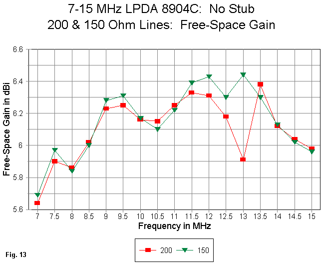
The free-space gain curves of Fig. 13 compare 200-Ohm and 150-Ohm versions of the tapered-element-diameter version of our basic LPDA design. What we find in these graphs is--at the gain levels appropriate to the design change--essentially the same as with the basic 8904 model. Higher gain peaks are accompanied by deeper valleys. Moreover, pay especial attention to the frequency region between 12.5 and 13 MHz. One might get the impression that only a mild dip in gain occurs at 12.5 MHz, followed by a rise on the way to 13 MHz. In fact, as a detailed (0.1 MHz) sweep might show, the dip goes much deeper before it starts back upward toward the mark it reaches at 13 MHz.
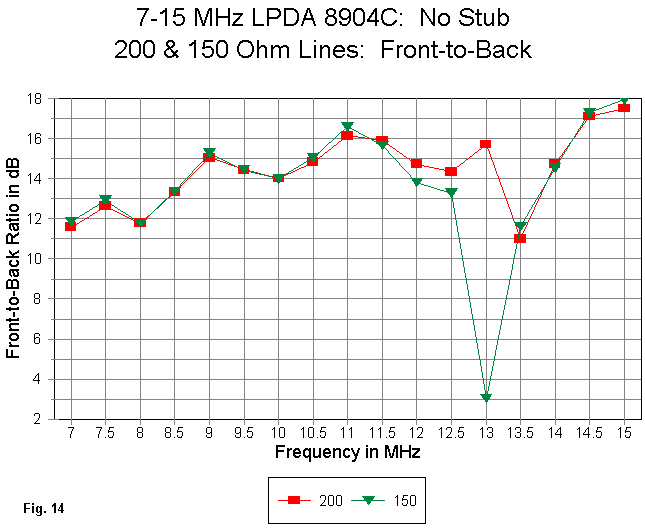
The front-to-back curves in Fig. 14 tend to replicate the results we obtained earlier. 13 MHz in this profile is a disaster of harmonic operation of the rearward elements. For the remainder of the curve, the lower impedance phaseline does yield on average a slightly higher front-to- back ratio.
These notes are, of course, predicated on the design goal of the exercise to obtain smooth performance of the highest attainable levels across the passband. Therefore, the gain and front-to-back ratio problems in the critical frequency region for this design have great weight. If one only wished to operate on 40, 30, and 20 meters, performance in the critical frequency region would likely be of little or no concern.
In this section we are bypassing concern for the VSWR curves, basically because for each model, there is a reference impedance that will yield values under 2:1 throughout to pass band. For 8904-200, the reference value is 90 Ohms, while for 8904-150, the value is 65 Ohms. For 8904C-200, the reference value is 90 Ohms, while for 8904C-150, the value is 75 Ohms. The trend is obvious: as we lower the phaseline impedance, the reference source impedance decreases.
What we have not shown--basically because graphing the phenomenon clearly is difficult--is the relative behavior of resistance and reactance as they compose the impedance. For the most part within the design passband, when the resistance reaches either its uppermost value or lowermost value, the reactance tends to be very low. At the median value of resistance, the reactance tends to be the highest. Hence, for a given reference impedance taken at about the median resistance value, the SWR level tends to be stable.
With very high values of Tau and optimum Sigma, the resistance value may change only by a few Ohms across the best operating range of the array. Likewise, the reactance will also vary little, yielding a very low SWR relative to a reference impedance. But even the longest LPDAs are not immune to changes in impedance, especially at the upper end of the passband.
Short-boom LPDAs tend to show the widest variation in both resistance and reactance. For example, the basic 8904 model with 1" diameter elements showed a resistance as high as 149 Ohms and as low as 51 Ohms. These are not the absolute peak values, but only the high and low that appeared within the boundaries of our limited profiles. In fact, the two values appeared at 14 and 15 MHz, with highs and lows hitting 120 and 60 Ohms, respectively, at lower frequencies in the passband.
The reactance range for 8904, as recorded in the profile, was +36 Ohms inductive and -52 Ohms capacitive. Capacitive reactance entries outnumbered inductive reactance entries, suggesting that this particular design has a median value that is inherently capacitively reactive.
To serve as a contrast, let me note once more the 434' LPDA design that covers 7 to 15 MHz with a Tau of .96 and a Sigma of 0.18 (optimal by calculation). The resistance rises above 69 Ohms only once, at 14.5 MHz, where it reaches 74 Ohms. The lowest profiled values is 57 Ohms, for a maximum range of 17 Ohms. If we exclude the 15 MHz reactance value of -33 Ohms, then the range of values across the rest of the passband runs from a low of j-4 Ohms to a high of j-17 Ohms, a mere 13 Ohms. And the reactance was capacitive throughout the profiled range. Such performance is largely unavailable to the short-boom LPDA designer.
Before we depart the strategy of reducing phaseline impedance to improve performance of a design with a set value of Tau and Sigma, let's look briefly at the model 8904C with a stub. This time, we shall compare three phaseline impedances: 200, 150, and 100 Ohms. As with the other exercises in reducing phaseline impedance, the reference impedance for the 2:1 SWR curve also goes down. The 200-Ohm model uses a reference impedance of 90 Ohms. The 150-Ohm version uses 75 Ohms, while the 100-Ohm model uses 55 Ohms (but might have used 50 Ohms as well).
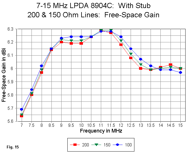
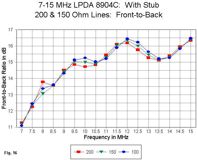
Fig. 15 presents the free-space gain curves of the three variant models. The 100-Ohm model has the highest average gain of the group, although its gain falls at the upper end of the passband. The front-to-back ratio curves in Fig. 16 also show the general, but slight, superiority of the 100-Ohm model.
The general equality of values from an operational standpoint raises the question of why one would move to the 100-Ohm phase line value. There is more than one reason. First, the 100-Ohm model can be fed directly with 50-Ohm feedline, without a matching device. Second, phaselines in the vicinity of 100 Ohms can be fabricated from square metal stock, thus allowing the phaseline also to serve as the boom to support the antenna elements. From a structural perspective, then, there are good reasons for lowering the phaseline impedance even when the performance improvements are marginal or non-existent.
However, a lower phaseline value requires a shorter stub than a higher phaseline value if we are to control the critical frequency region of the passband. The 200-Ohm model used a 6" stub, while the 150-Ohm version used a 3" stub, both 600 Ohm lines. The 100-Ohm model used a 1" stub, essentially a short circuit jumper at the rear of the double boom phaseline. Despite tailoring the stub length to the phaseline impedance value, the stub proved less effective in reducing harmonic operation of the rear elements as the phaseline impedance decreased. Fig. 17 shows the remnant harmonic current distribution and magnitude for the 100-Ohm model at 13.25 MHz.
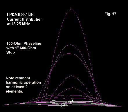
The design goal with lower impedance phaselines is rarely to wholly eliminate harmonic operation of the rear elements. Rather, the aim is to reduce such currents to levels that permit relatively normal performance levels relative to the overall curves, as well as azimuth patterns that can be called "well-behaved." The current distribution and magnitude on the rear elements of Fig. 17, while higher than for the 200-Ohm model at the same frequency, still do not significantly distort the main pattern.
Nevertheless, the overall gain pattern of Fig. 15 might be considered a bit distressing from the design perspective. The gain falls off at both ends of the passband, with the lower end of the band a special concern. Is there a way to elevate the gain at the band edges without losing significant amounts of gain in the mid-passband region?
The resulting LPDA appears in the following description.
8904EX.EZ                      EZNEC/4  ver. 2.5

6.4-17 MHz .89/.04                           10-09-1999     07:41:09

Frequency = 14  MHz.

Wire Loss: Aluminum -- Resistivity = 4E-08 ohm-m, Rel. Perm. = 1

              --------------- WIRES ---------------

Wire Conn.--- End 1 (x,y,z : in)  Conn.--- End 2 (x,y,z : in)  Dia(in) Segs

1          0.000,-470.47,  0.000         0.000,470.475,  0.000 1.00E+00  39
2         75.276,-418.72,  0.000        75.276,418.723,  0.000 1.00E+00  35
3        142.272,-372.66,  0.000       142.272,372.663,  0.000 1.00E+00  31
4        201.898,-331.67,  0.000       201.898,331.670,  0.000 1.00E+00  27
5        254.965,-295.19,  0.000       254.965,295.187,  0.000 1.00E+00  25
6        302.195,-262.72,  0.000       302.195,262.716,  0.000 1.00E+00  23
7        344.229,-233.82,  0.000       344.229,233.817,  0.000 1.00E+00  19
8        381.640,-208.10,  0.000       381.640,208.097,  0.000 1.00E+00  17
9        414.936,-185.21,  0.000       414.936,185.207,  0.000 1.00E+00  15
10       444.569,-164.83,  0.000       444.569,164.834,  0.000 1.00E+00  13
11       470.942,-146.70,  0.000       470.942,146.702,  0.000 1.00E+00  13
12       494.415,-130.56,  0.000       494.415,130.565,  0.000 1.00E+00  11

              -------------- SOURCES --------------

Source    Wire      Wire #/Pct From End 1    Ampl.(V, A)  Phase(Deg.)  Type
          Seg.     Actual      (Specified)

1           6    12 / 50.00   ( 12 / 50.00)      0.707       0.000       V

No loads specified

                -------- TRANSMISSION LINES ---------

Line  Wire #/% From End 1   Wire #/% From End 1    Length     Z0   Vel Rev/
      Actual  (Specified)   Actual  (Specified)              Ohms Fact Norm

1    1/50.0  (  1/50.0)    2/50.0  (  2/50.0)  Actual dist  200.0  1.00  R
2    2/50.0  (  2/50.0)    3/50.0  (  3/50.0)  Actual dist  200.0  1.00  R
3    3/50.0  (  3/50.0)    4/50.0  (  4/50.0)  Actual dist  200.0  1.00  R
4    4/50.0  (  4/50.0)    5/50.0  (  5/50.0)  Actual dist  200.0  1.00  R
5    5/50.0  (  5/50.0)    6/50.0  (  6/50.0)  Actual dist  200.0  1.00  R
6    6/50.0  (  6/50.0)    7/50.0  (  7/50.0)  Actual dist  200.0  1.00  R
7    7/50.0  (  7/50.0)    8/50.0  (  8/50.0)  Actual dist  200.0  1.00  R
8    8/50.0  (  8/50.0)    9/50.0  (  9/50.0)  Actual dist  200.0  1.00  R
9    9/50.0  (  9/50.0)   10/50.0  ( 10/50.0)  Actual dist  200.0  1.00  R
10  10/50.0  ( 10/50.0)   11/50.0  ( 11/50.0)  Actual dist  200.0  1.00  R
11  11/50.0  ( 11/50.0)   12/50.0  ( 12/50.0)  Actual dist  200.0  1.00  R
12   1/50.0  (  1/50.0)  Short ckt (Short ck)    6.000 in   600.0  1.00

Ground type is Free Space
Immediately apparent is the fact that the new LPDA design with which we hope to achieve performance extensions is about 6.3' longer than our standard model (41.2' vs. 34.9'), and it has two more elements. It is in every way a larger antenna. Now we can ask what we gain for our trouble.
To set the comparison on fair ground, both model will use our original 1" diameter elements and the standard 200-Ohm inter-element phaseline. Hence, the standard of comparison will be the antenna described at the beginning of this part. To smooth the curves, a 6" 600-Ohm stub has been installed at the center of the longest element of each antenna. Since we have established that virtually all of the models with which we are dealing have decent SWR profiles across the 7 to 15 MHz passband, we shall omit these curves. The original 10-element model is referenced to 90 Ohms, while the new extended model is referenced to 100 Ohms. With this in mind, we can look at the free-space gain and front-to-back curves in search on improvements.
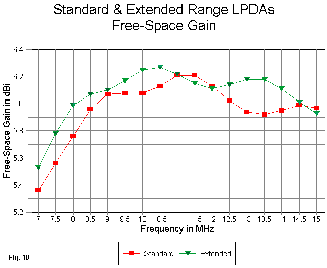
Fig. 18 shows us what we gained in the battle for gain: only a little. The extended LPDA improves the low-end gain by under 0.2 dB. There are higher gain peaks along the curve, especially in the 12.5 to 14 MHz region, but the gain is actually lower than that of the original model at the upper passband limit.
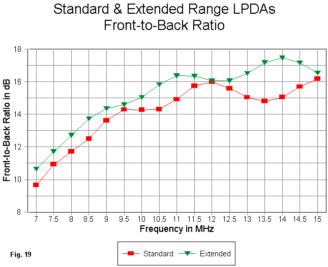
Our most consistent gain is in front-to-back ratio, as shown in Fig. 19. Except for the significant improvement in the 13 to 14.5 MHz region, the increase tends to average about 1 dB. It is dubious whether this improvement would be operationally significant--and whether it would justify the added complexity of the resulting design.
If we recall that out goal was to improve performance at the passband edges rather than seeking an overall improvement, we have gained very little from the first effort to improve performance. We need a different strategy.
One commercial strategy appears to be varying the Tau used for element lengths while preserving a constant Tau for element spacing. There are proprietary algorithms used for such designs which may go under the name of "circular" design. I have also seen an interesting spot application of the principle by Eric Gustafson, N7CL. The general principle is sound, and might even be applied also to element spacing, although I have not tried it there.
I have redesigned the original 8904 model (with stub) according to the circular-Tau principle, so let's examine the new element lengths as a basis for explaining the procedure and discovering why it might be called circular.
8906CIR.EZ                      EZNEC/4  ver. 2.5

6.8-15 MHz .89/.04                           10-09-1999     10:43:05

Frequency = 7  MHz.

Wire Loss: Aluminum -- Resistivity = 4E-08 ohm-m, Rel. Perm. = 1

              --------------- WIRES ---------------

Wire Conn.--- End 1 (x,y,z : in)  Conn.--- End 2 (x,y,z : in)  Dia(in) Segs

1          0.000,-424.00,  0.000         0.000,424.000,  0.000 1.00E+00  31
2         70.848,-386.30,  0.000        70.848,386.300,  0.000 1.00E+00  27
3        133.903,-349.00,  0.000       133.903,349.000,  0.000 1.00E+00  25
4        190.021,-312.16,  0.000       190.021,312.160,  0.000 1.00E+00  23
5        239.967,-277.82,  0.000       239.967,277.823,  0.000 1.00E+00  19
6        284.419,-247.26,  0.000       284.419,247.262,  0.000 1.00E+00  17
7        323.981,-221.00,  0.000       323.981,221.000,  0.000 1.00E+00  15
8        359.191,-198.00,  0.000       359.191,198.000,  0.000 1.00E+00  13
9        390.528,-181.00,  0.000       390.528,181.000,  0.000 1.00E+00  13
10       418.418,-170.00,  0.000       418.418,170.000,  0.000 1.00E+00  11

              -------------- SOURCES --------------

Source    Wire      Wire #/Pct From End 1    Ampl.(V, A)  Phase(Deg.)  Type
          Seg.     Actual      (Specified)

1           6    10 / 50.00   ( 10 / 50.00)      0.707       0.000       V

No loads specified

                -------- TRANSMISSION LINES ---------

Line  Wire #/% From End 1   Wire #/% From End 1    Length     Z0   Vel Rev/
      Actual  (Specified)   Actual  (Specified)              Ohms Fact Norm

1    1/50.0  (  1/50.0)    2/50.0  (  2/50.0)  Actual dist  200.0  1.00  R
2    2/50.0  (  2/50.0)    3/50.0  (  3/50.0)  Actual dist  200.0  1.00  R
3    3/50.0  (  3/50.0)    4/50.0  (  4/50.0)  Actual dist  200.0  1.00  R
4    4/50.0  (  4/50.0)    5/50.0  (  5/50.0)  Actual dist  200.0  1.00  R
5    5/50.0  (  5/50.0)    6/50.0  (  6/50.0)  Actual dist  200.0  1.00  R
6    6/50.0  (  6/50.0)    7/50.0  (  7/50.0)  Actual dist  200.0  1.00  R
7    7/50.0  (  7/50.0)    8/50.0  (  8/50.0)  Actual dist  200.0  1.00  R
8    8/50.0  (  8/50.0)    9/50.0  (  9/50.0)  Actual dist  200.0  1.00  R
9    9/50.0  (  9/50.0)   10/50.0  ( 10/50.0)  Actual dist  200.0  1.00  R
10   1/50.0  (  1/50.0)  Short ckt (Short ck)    6.000 in   600.0  1.00

Ground type is Free Space
In this sample application, I chose to preserve the lengths of elements 4, 5, and 6. These element lengths are related by a Tau of 0.89. The rear three elements and forward 4 elements use a variable Tau that might roughly approximate a curve described by a circle.
Elements 3 and 7 increase the value of Tau by about 0.05% (multiply 0.89 by 1.005). The 7th element length is thus about 0.894 times the 6th element length. For the rearward elements, we use the inverse of Tau, or about 1.118 to obtain the new length of element 3 from element 4. Then, we increase Tau once more, this time by a slightly greater amount, say 1%. Hence, we take our new value of Tau and multiply by 1.01 to get about 0.903. The 8th element length is about 0.903 the length of the new 7th element, while the 2nd element is about 1.107 times the length of the new 3rd element. The next Tau value can be about 1.5% or so the values just established, or about 0.917, and so on until we run out of elements in either direction, or until we reach about 0.96 for Tau.
The elements shown use rounded lengths for our experiment, since we are only testing the principle of circular Tau. Moreover, the shortening of the rearmost element was halted just at the point where the SWR curve (referenced to 95 Ohms) remained within the 2:1 limit without changing the 6" stub. This called for a longer than ideal length for the rear element. You may experiment with changing the stub to effect further improvements while retaining a usable SWR profile. In fact, you may also wish to apply any of the other strategies we have so far discussed to our circular Tau model. Remember that we are illustrating techniques only. We are not striving for a final design to build.
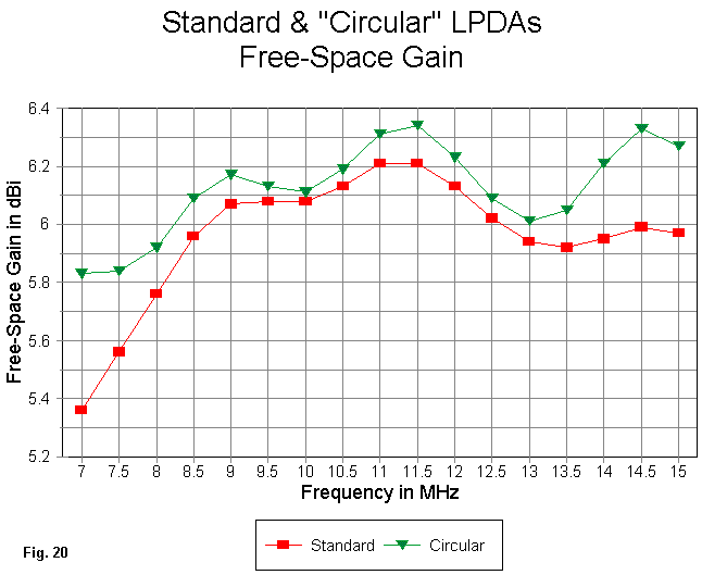
However, circularizing Tau brings us dramatically toward that goal, as witnessed by Fig. 20. The gain at both passband edges shows a dramatic upturn: about 0.5 dB at the low end and 0.3 dB at the upper end. The overall curve is slightly stronger than that of the original model, but the chief improvement is more consistent gain across the entire spectrum.
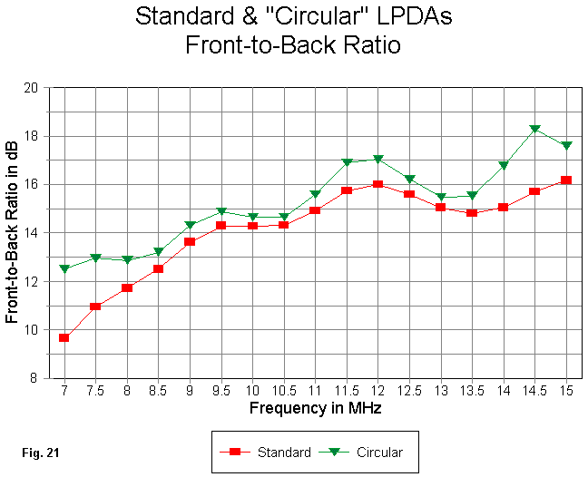
The improved front-to-back curve, shown in Fig. 21, would also be a marginal improvement were it not for passband edge improvements. At 7 MHz, the improvement is nearly 3 dB, an amount that approaches operational notice. Unlike the extended range LPDA design, these improvements add nothing to the length of the array, the number of elements, or the weight. Hence, pursuit of this strategy--perhaps in conjunction with larger element diameters, stub refinements, and a lower inter-element phaseline characteristic impedance to obtain a direct 50-Ohm match across the passband--might be a useful exercise for anyone wishing to perfect old 8904.
There is a technique that will overcome this tendency. Let's specify that the design will use the standard 200-Ohm inter-element phaseline as a basic factor. This impedance may not offer the highest gain at every point in the passband, but it helps to suppress any instabilities in pattern shape occasioned by harmonic operation of longer elements.
Instead of bringing the 200-Ohm line all the way to the shortest element, let's taper the characteristic impedance until it reaches a lower value at the feedline junction. The exact lower limit of the tapered Zo will depend on the natural reference impedance for the antenna, but something between 80 and 150 Ohms will do for most designs. We need not taper the impedance for the entire length of the LPDA, but only for about the forward-most 15% of the elements. Since this value amounts to about 1.5 elements for our standard demonstration model, it is inconvenient to demonstrate the technique on a small LPDA without introducing some modeling techniques that would obscure the point.
However, I have mentioned, in this part and the last, a long LPDA (434') that uses 27 elements with a Tau of 0.96 (maximum recommended value) and a Sigma of 0.18 (optimum value). This is a convenient model to use for the demonstration for several reasons. First, it has many elements, and the tapered phaseline can be implemented in small steps that simulate the taper. Second, the design, created by standard calculations, has some other features of interest.
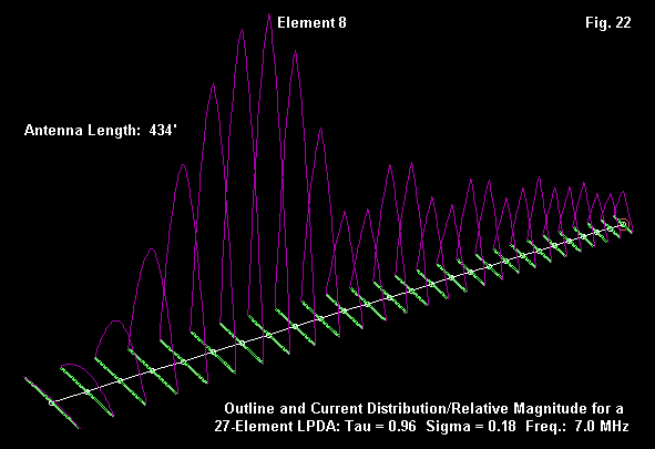
Fig. 22 shows the outline of the antenna. Remember that the elements are within the same length range used by those of the short LPDA we have been studying. Thus, the scaled sketch gives a true picture of the antenna's overall length.
Of great interest is the current distribution and relative magnitude shown in the graphic. Of first note is the element showing the highest current in this 7 MHz view. As we increase Tau, we increase the number of elements and, with it, the inter-element coupling. Hence, we should for any high- Tau design also see the low-frequency high-current element move forward in the array. In this array, we might remove the rear-most element with little ill effect.
Of second note is the number of very active elements that affect the pattern formation of the array at even the lowest frequency. For all but one element, the current levels are non-negligible. We should expect from this array a good gain, but more especially, an astounding front-to-back ratio, regardless of whether we are concerned with 180-degree, worst-case, or front-to-rear ratios.
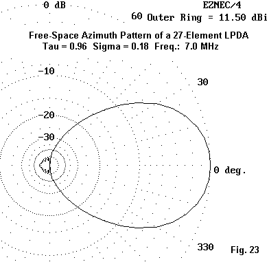
Fig. 23 confirms our suspicions. More dramatic than the 11.5 dBi free- space gain of the array is the truly insignificant radiation to the rear. It should be no mystery why many commercial and government shortwave stations have gone to sizable LPDA arrays and given up many of the older wire arrays that once covered hillsides.
In case you wish to operate a (duly-licensed) multi-frequency shortwave station between 7 and 15 MHz, here is the model description, using 1" diameter elements and requiring no stub.
9618.EZ                      EZNEC/4  ver. 2.5

.96/.18 6.8-15 MHz 27 el                     10-09-1999     15:57:49

Frequency = 7  MHz.

Wire Loss: Aluminum -- Resistivity = 4E-08 ohm-m, Rel. Perm. = 1

              --------------- WIRES ---------------

Wire Conn.--- End 1 (x,y,z : in)  Conn.--- End 2 (x,y,z : in)  Dia(in) Segs

1          0.000,-442.80,  0.000         0.000,442.800,  0.000 1.00E+00  31
2        318.816,-425.09,  0.000       318.816,425.088,  0.000 1.00E+00  31
3        624.879,-408.08,  0.000       624.879,408.084,  0.000 1.00E+00  29
4        918.700,-391.76,  0.000       918.700,391.761,  0.000 1.00E+00  29
5        1200.77,-376.09,  0.000       1200.77,376.091,  0.000 1.00E+00  27
6        1471.55,-361.05,  0.000       1471.55,361.047,  0.000 1.00E+00  25
7        1731.51,-346.61,  0.000       1731.51,346.605,  0.000 1.00E+00  25
8        1981.06,-332.74,  0.000       1981.06,332.741,  0.000 1.00E+00  23
9        2220.64,-319.43,  0.000       2220.64,319.431,  0.000 1.00E+00  23
10       2450.63,-306.65,  0.000       2450.63,306.654,  0.000 1.00E+00  23
11       2671.42,-294.39,  0.000       2671.42,294.388,  0.000 1.00E+00  21
12       2883.38,-282.61,  0.000       2883.38,282.612,  0.000 1.00E+00  21
13       3086.86,-271.31,  0.000       3086.86,271.308,  0.000 1.00E+00  19
14       3282.20,-260.46,  0.000       3282.20,260.456,  0.000 1.00E+00  19
15       3469.73,-250.04,  0.000       3469.73,250.037,  0.000 1.00E+00  17
16       3649.75,-240.04,  0.000       3649.75,240.036,  0.000 1.00E+00  17
17       3822.58,-230.43,  0.000       3822.58,230.434,  0.000 1.00E+00  17
18       3988.49,-221.22,  0.000       3988.49,221.217,  0.000 1.00E+00  15
19       4147.77,-212.37,  0.000       4147.77,212.368,  0.000 1.00E+00  15
20       4300.67,-203.87,  0.000       4300.67,203.874,  0.000 1.00E+00  15
21       4447.46,-195.72,  0.000       4447.46,195.719,  0.000 1.00E+00  15
22       4588.38,-187.89,  0.000       4588.38,187.890,  0.000 1.00E+00  13
23       4723.66,-180.37,  0.000       4723.66,180.374,  0.000 1.00E+00  13
24       4853.53,-173.16,  0.000       4853.53,173.159,  0.000 1.00E+00  13
25       4978.21,-166.23,  0.000       4978.21,166.233,  0.000 1.00E+00  11
26       5097.89,-159.58,  0.000       5097.89,159.584,  0.000 1.00E+00  11
27       5212.79,-153.20,  0.000       5212.79,153.200,  0.000 1.00E+00  11

              -------------- SOURCES --------------

Source    Wire      Wire #/Pct From End 1    Ampl.(V, A)  Phase(Deg.)  Type
          Seg.     Actual      (Specified)

1           6    27 / 50.00   ( 27 / 50.00)      0.707       0.000       V

No loads specified

                -------- TRANSMISSION LINES ---------

Line  Wire #/% From End 1   Wire #/% From End 1    Length     Z0   Vel Rev/
      Actual  (Specified)   Actual  (Specified)              Ohms Fact Norm

1    1/50.0  (  1/50.0)    2/50.0  (  2/50.0)  Actual dist  200.0  1.00  R
2    2/50.0  (  2/50.0)    3/50.0  (  3/50.0)  Actual dist  200.0  1.00  R
3    3/50.0  (  3/50.0)    4/50.0  (  4/50.0)  Actual dist  200.0  1.00  R
4    4/50.0  (  4/50.0)    5/50.0  (  5/50.0)  Actual dist  200.0  1.00  R
5    5/50.0  (  5/50.0)    6/50.0  (  6/50.0)  Actual dist  200.0  1.00  R
6    6/50.0  (  6/50.0)    7/50.0  (  7/50.0)  Actual dist  200.0  1.00  R
7    7/50.0  (  7/50.0)    8/50.0  (  8/50.0)  Actual dist  200.0  1.00  R
8    8/50.0  (  8/50.0)    9/50.0  (  9/50.0)  Actual dist  200.0  1.00  R
9    9/50.0  (  9/50.0)   10/50.0  ( 10/50.0)  Actual dist  200.0  1.00  R
10  10/50.0  ( 10/50.0)   11/50.0  ( 11/50.0)  Actual dist  200.0  1.00  R
11  11/50.0  ( 11/50.0)   12/50.0  ( 12/50.0)  Actual dist  200.0  1.00  R
12  12/50.0  ( 12/50.0)   13/50.0  ( 13/50.0)  Actual dist  200.0  1.00  R
13  13/50.0  ( 13/50.0)   14/50.0  ( 14/50.0)  Actual dist  200.0  1.00  R
14  14/50.0  ( 14/50.0)   15/50.0  ( 15/50.0)  Actual dist  200.0  1.00  R
15  15/50.0  ( 15/50.0)   16/50.0  ( 16/50.0)  Actual dist  200.0  1.00  R
16  16/50.0  ( 16/50.0)   17/50.0  ( 17/50.0)  Actual dist  200.0  1.00  R
17  17/50.0  ( 17/50.0)   18/50.0  ( 18/50.0)  Actual dist  200.0  1.00  R
18  18/50.0  ( 18/50.0)   19/50.0  ( 19/50.0)  Actual dist  200.0  1.00  R
19  19/50.0  ( 19/50.0)   20/50.0  ( 20/50.0)  Actual dist  200.0  1.00  R
20  20/50.0  ( 20/50.0)   21/50.0  ( 21/50.0)  Actual dist  200.0  1.00  R
21  21/50.0  ( 21/50.0)   22/50.0  ( 22/50.0)  Actual dist  200.0  1.00  R
22  22/50.0  ( 22/50.0)   23/50.0  ( 23/50.0)  Actual dist  175.0  1.00  R
23  23/50.0  ( 23/50.0)   24/50.0  ( 24/50.0)  Actual dist  150.0  1.00  R
24  24/50.0  ( 24/50.0)   25/50.0  ( 25/50.0)  Actual dist  125.0  1.00  R
25  25/50.0  ( 25/50.0)   26/50.0  ( 26/50.0)  Actual dist  100.0  1.00  R
26  26/50.0  ( 26/50.0)   27/50.0  ( 27/50.0)  Actual dist   80.0  1.00  R

Ground type is Free Space
The model description actually shows the modifications in transmission lines 22-26 for the tapered impedance technique. Returning all of the lines to 200 Ohms would show the basic model. Note that the impedance increases in 20-25 Ohm steps from a feedpoint junction value of 80 Ohms up to the standard value for the remainder of the line. The impedance- tapering technique does have some useful effects on the performance of the array at the upper end of the passband.
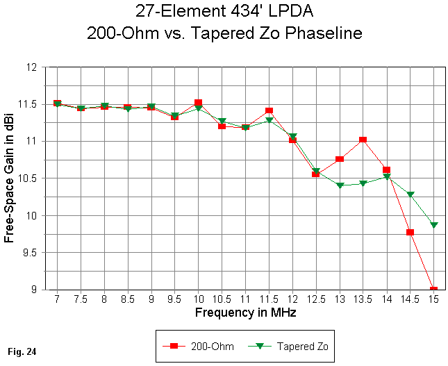
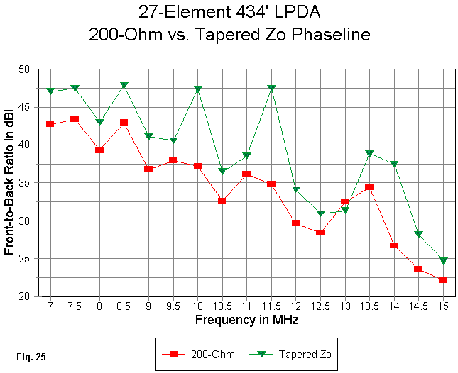
In Fig. 24, we can see the smoothing of the gain curve above 12.5 MHz. What we lose in the 13.5 MHz peak of the original we more than make up in the improved gain at 14.5 and 15 MHz. The front-to-back curve in Fig. 25 shows improvements for the tapered-impedance line model, although there are sharper peaks. Only at 13 MHz does the original model show a higher front- to-back ratio, but I suspect that adding a stub to the original might smooth its curve in this region. However, I did not add a 6" stub to the 434' array. Nor did I apply a circular Tau correction to the forward elements, although such a trial might show whether the value of Tau can be usefully raised above 0.96 to improve upper frequency performance. Implementing this last possible strategy might have obscured the effects of the tapered-impedance phaseline.
We noted earlier that this high-Tau array has extended low-frequency capability. In fact, the array performance does not decrease significantly until below 6.5 MHz, and it is still usable at 6 MHz, where the gain is above 10 dBi and the front-to-back ratio above 20 dB. Therefore, the following SWR curves encompass the range of 6 to 16 MHz.
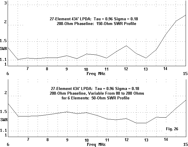
The upper portion of Fig. 26 shows the 150-Ohm SWR curve for the model with a uniform 200-Ohm phase line. For a very large portion of the passband, the 150-Ohm reference is clearly the natural impedance of the antenna. However, at the upper end of the spectrum, the resistive component of the impedance descends toward 80 Ohms, while the reactance climbs to exceed 100 Ohms at the passband limit.
The lower curve uses a 50-Ohm reference. The entire curve is well below the 2:1 limit we set somewhat arbitrarily as the goal. By the use of the tapered-impedance phase line, we electrically simplify the array by eliminating the need for a wide-band matching device at the feedpoint, should we choose to feed the array with standard 50-Ohm coaxial cable.
Moreover, we have only demonstrated the techniques. We did not seek to arrive at a final design that we might build. The techniques can be combined to yield a final design, but just which combination and to what degree each technique might be used would form a set of design decisions based on having a clear set of operational goals. Without such goals, but only our general guideline, any claim that one of the design results within the demonstration was "best" would be foolish.
Moreover, we chose a basic model that clearly could stand improvement. Old 8904 is a modest LPDA design, not necessarily the best, even for its boom length. Other combinations of Tau and Sigma that yield the same boom length might prove initially superior--or more amenable to some of the improvement techniques. 8904 was simply handy because it permitted the techniques to be demonstrated.
Likewise, the frequency range was semi-arbitrary, since it avoided any possible controversy that might surround comparating LPDAs that have been built for the upper HF region. Nevertheless, the models used are easily scaled by a factor of 2 (including element diameter) for the 14 to 30 MHz range. Only the losses of the aluminum elements will shift any of the modeled results--and any shift will be slight.
With all of these qualifications, I still hope that sorting out the various techniques available to improve the performance of basic LPDA designs is useful. The exercise may go some distance toward improving our understanding of LPDAs in all their major variations.
Updated 10-11-99. © L. B. Cebik, W4RNL. Data may be used for
personal purposes, but may not be reproduced for publication in print or
any other medium without permission of the author.